ADVANCED NANOSTRUCTURED MATERIALS PROCESSING AND CHARACTERIZATION EQUIPMENTS
Project Title: “DEVELOPMENT OF THE RESEARCH INFRASTRUCTURE FOR THE PROCESSING AND CHARACTERIZATION OF ADVANCED NANOSTRUCTURED MATERIALS”
Acronym: PC-MAN
Contract No. 122/2007
Financed in the frame of PN II - CAPACITIES Programme/Module I
CONDIŢII de ACCES:
the facilities are made available for parties by programation based on request;
access conditions/costs - based on invoice/negociated costs in function of the requested service and allocated time.
CONTACT:
Prof. Dr. Horia CHIRIAC, General Director (hchiriac@phys-iasi.ro)
Dr. Nicoleta LUPU, Head of "Magnetic Materials and Devices" Department (nicole@phys-iasi.ro)
Tel: +40 232 43 06 80
Fax: +40 232 23 11 32
![]()
AVAILABLE EQUIPMENTS:
![]() Electron beam lithography system XENOS XP G2
Electron beam lithography system XENOS XP G2
![]() Alpha
Step IQ surface profiler for thin films thickness
measurements
Alpha
Step IQ surface profiler for thin films thickness
measurements
![]() Focused
Ion Beam - Scanning Electron Microscope
Carl Zeiss CrossBeam NEON40EsB FIB-SEM
Focused
Ion Beam - Scanning Electron Microscope
Carl Zeiss CrossBeam NEON40EsB FIB-SEM
![]()
Electron beam lithography system XENOS XP G2
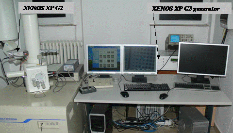
JEOL JSM 6390A Scanning Electron Microscope equipped with
electron beam lithography system XENOS XP G2.
The electron beam lithography system is a complex experimental system used for geometrical nanostructuring activities. The lithography nanostructuring technique of a material’s surface consists in scanning the surface with a focused electron beam, surface which has been previously covered with a polymeric (e.g. e - beam resist) which is sensitive to the electron beam action. In comparison with the optical lithography technique, the electron beam lithography technique permits high resolution geometrical structuring of materials due to the small value of the wavelength (< 1 Ǻ), specific for the accelerated electrons at voltages in the range 10-50 keV.
Using the electron beam lithography technique, the planar geometry of materials can be achieved, which are subsequently used for:
various structures/geometries: rezistive, inductive, etc;
Technical characteristics of the XENOS XP G2 electron beam lithography system:
![]()
The Alpha Step IQ surface profiler used for topological characterization and thin films thickness measurements
Is a high resolution equipment which can measure the thin film thickness with a resolution of 0.1 Ǻ.
The Alpha Step IQ can determine the bi-dimensional topographic analysis of the samples’ surface (thin films, wafers, micro- and nanoelectromechanical systems - MEMS and NEMS, nano or microporous ceramic or polymeric membranes, etc).
Alpha Step IQ gives also information on the surface roughness of materials in planar structures.
Owing to the high resolution, the Alpha Step IQ can be used for the calibration of other equipments in NIRDTP Iasi employed to monitor the thin film thickness during the preparation process, vacuum or electrochemical deposition, such as:
- FTM6 Film Thickness Monitor (0.1 nm resolution);
- INFICON XTC/3M Deposition Controller (0.5% accuracy,: ± 2.5 ppm 0-500C frequency accuracy);
- QCM200 Quartz Crystal Microbalance.
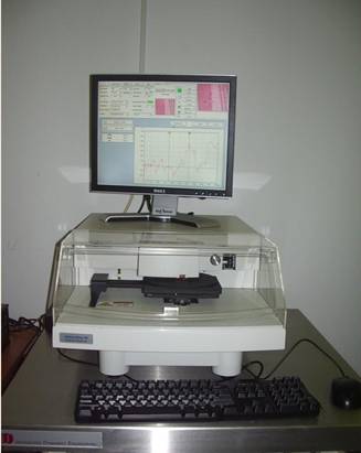
Alpha Step IQ surface profiler.
The technical characteristics of the Alpha Step IQ surface profiler used for topological characterization and thin films thickness measurements are:
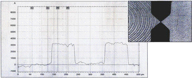
Thickness profile for a metallic resistive thin film structured in a circular shape.
With the view of the optimization of the thickness measurement process, mainly for ultrathin thin films, the Alpha Step IQ has been positioned on an antivibrating table with the natural vibrating frequency, horizontally and vertically, of 2.5 Hz.
![]()
CrossBeam Focused Ion Beam/Scanning Electron Microscope Carl Zeiss NEON40EsB FIB-SEM
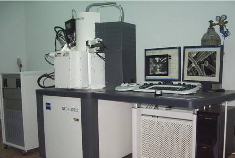
FIB/FE-SEM
CrossBeam
Carl Zeiss
NEON 40 EsB
equipped
with
EDS module
Is a state of the art technological facility, unique in Romania, used for complex ion beam micro and nanoprocessing/treatment of materials such as:
The Focused Ion Beam (FIB) system uses a high focused Galium (Ga) ion beam to locally heat the metal or to evaporate a material for the deposition on a well defined area of micrometer/nanometer size.
Using various gases or organic compounds, the FIB can be used for the corrosion selectively and rapidly any type of material, this facility being useful for a series of special applications such as: (i) preparation of cross sections for the study of interfaces in multilayer systems; (ii) preparation of samples for Transmission Electron Microscopy (TEM); (iii) preparation of microsamples by microprocessing of bulk materials, etc.
The FIB/FE-SEM CrossBeam NEON 40 EsB is a complex system used for the nanoprocessing and characterisation of nanomaterials which consists of:
1) ions gun for FIB function;
2) electrons gun for High Resolution Field Emission Electron Scanning Microscopy, which allows in-situ visualization of the structures prepared by ions etching/deposition;
3) EDS detector for qualitative and quantitative determination of materials composition.
The system is complementarly used for the compositional and morphological/topological analysis of materials by Field Emission Scanning Electron Microscopy (FE-SEM) and X-ray energy dispersive spectrometry (EDS).
The technical characteristics of the CrossBeam FIB-SEM NEON 40 EsB are :
![]()